The Car Hacker's Handbook: A Guide for the Penetration Tester - Craig Smith (2016)
Chapter 8. ATTACKING ECUS AND OTHER EMBEDDED SYSTEMS

The ECU is a common target of reverse engineering, sometimes referred to as chip tuning. As mentioned in Chapter 7, the most popular ECU hack is modifying the fuel map to alter the balance of fuel efficiency and performance in order to give you a higher-performance vehicle. There’s a large community involved with these types of modifications, and we’ll go into more detail on firmware modifications like this in Chapter 13.
This chapter will focus on generic embedded-system methods of attack as well as side-channel attacks. These methodologies can be applied to any embedded system, not just to the ECU, and they may even be used to modify a vehicle with the help of aftermarket tools. Here, we’ll focus on debugging interfaces for hardware as well as performing side-channel analysis attacks and glitching attacks.
NOTE
To get the most out of this chapter, you should have a good understanding of basic electronics, but I’ve done my best to explain things within reason.
Analyzing Circuit Boards
The first step in attacking the ECU or any embedded system in a vehicle is to analyze the target circuit board. I touched upon circuit board analysis in Chapter 7, but in this chapter, I’ll go into more detail about how electronics and chips work. I’ll introduce you to techniques that can be applied to any embedded system in the vehicle.
Identifying Model Numbers
When reversing a circuit board, first look at the model numbers of the microcontroller chips on the board. These model numbers can help you track down valuable information that can be key to your analysis. Most of the chips you’ll find on vehicle circuit boards are generic—companies rarely make custom ones—so an Internet search of a chip’s model number can provide you with the complete data sheet for that chip.
As mentioned in Chapter 7, you’ll sometimes run into custom ASIC processors with custom opcodes, especially in older systems, which will be harder to reprogram. When you encounter older chips like these, remove them from the board and plug them in to an EPROM programmer in order to read their firmware. You should be able to reprogram modern systems directly via debugging software, like JTAG.
Once you locate a data sheet, try to identify the microcontrollers and memory locations on each chip to determine how things are wired together and where to find diagnostic pins—a potential way in.
Dissecting and Identifying a Chip
If you can’t find a model number, sometimes all you’ll have to go on is the chip’s logo (after a while, you’ll find that you start to recognize chip logos) and a few of its product codes. The logo shown in Figure 8-1 is for STMicroelectronics. At the top of the chip is the model number—in this case, STM32F407—which may be hard to read because it’s engraved. Often, a light-up magnifier or a cheap USB microscope can prove very handy in reading these markings. Go to http://www.st.com/ to find the data sheet for the STM32F series chips, specifically the 407 variety. Much like VIN numbers, model numbers are often broken down into sections representing model number and different variations. There’s no standard for how to break down these numbers, however, and every manufacturer will represent their data differently.
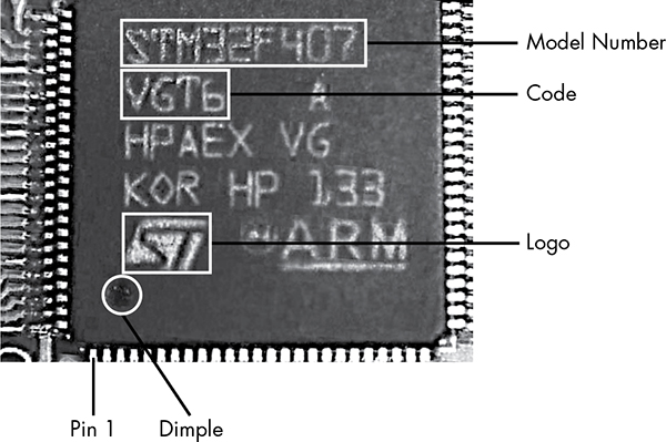
Figure 8-1: STM32 chipset identification
Below the chip’s model number is the code—in this case, VGT6—which tells you the specific features, such as USB support, available on the chip. If you look up the model number in conjunction with the ST code, you’ll learn that the STM32F407Vx series is an ARM Cortext M4 chip with support for Ethernet, USB, two CANs, and LIN as well as JTAG and Serial Wire Debug.
To determine the function of the various pins, scan the data sheet to find the package pinout diagrams, and look for the package that matches yours for pin count. For example, as you can see in Figure 8-1, each side of the chip has 25 pins for a total of 100, which matches the LQFP100 pinout in the data sheet shown in Figure 8-2.
Each chip will usually have a dot or dimple at pin 1 (see Figure 8-1), and once you identify pin 1, you can follow the pinout to determine each pin’s function. Sometimes you’ll find two dimples, but one should be slightly more pronounced.
Sometimes pin 1 on a chip is indicated by a cut-off corner. If you find nothing on a chip that allows you to identify pin 1, look for things you can identify. For example, if another chip on the board is a common CAN transceiver, you could use a multitool to trace the lines to figure out which pins it connects to. You could then reference the data sheet to see which side of the chip contains these CAN pins. To do this, put your multimeter in continuity mode. Once in continuity mode, it will beep if you touch both pins to the same trace, indicating that they’re connected. Once you’re able to identify just one pin, you can use that information together with the pinout to deduce the pin layout.
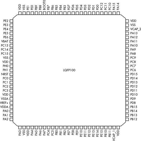
Figure 8-2: STM32F4 data sheet pinout
Debugging Hardware with JTAG and Serial Wire Debug
You can use a variety of debugging protocols to debug chips just as you do software. To determine which protocol your target chip supports, you’ll need to use the chip’s data sheet. You should be able to use a chip’s debugging port to intercept its processing and download and upload modifications to the chip’s firmware.
JTAG
JTAG is a protocol that allows for chip-level debugging and downloading and uploading firmware to a chip. You can locate the JTAG connections on a chip using its data sheet.
JTAGulator
You’ll often find pads on a chip’s circuit board that are broken out from the chip itself and that may give you access to the JTAG pins. To test the exposed pads for JTAG connections, use a tool like JTAGulator, shown in Figure 8-3. Plug all of the chip’s exposed pins in to the JTAGulator, and set the voltage to match the chip. JTAGulator should then find any JTAG pins and even walk the JTAG chain—a method of linking chips over JTAG—to see whether any other chips are attached.

Figure 8-3: JTAGulator with a Bus Pirate cable
JTAGulator supports either screw terminals or the use of a Bus Pirate cable (as in Figure 8-3) for probing. Both the JTAGulator and the Bus Pirate cable use a serial interface to configure and interact with a chip.
Debugging with JTAG
You can debug a chip with JTAG using just two wires, but it’s more common to use four or five pin connections. Of course, finding the JTAG connection is only the first step; usually, you’ll need to overcome additional protections that prevent you from just downloading the chip’s firmware in order to do anything interesting.
Developers will disable JTAG firmware via either software or hardware. When disabling JTAG in software, the programmer sets the JTD bit, which is usually enabled twice via software during runtime. If the bit it isn’t called twice within a short time, it’s not set. It’s possible to defeat a software protection like this by using a clock or power-glitching attack to skip at least one of these instructions. (We’ll discuss glitching attacks later in “Fault Injection” on page 148.)
The other way to disable JTAG on a chip is to attempt to permanently disable programming by setting the JTAG fuse—OCDEN and JTAGEN—and thereby disabling both registers. This is harder to bypass with glitch attacks, though voltage glitching or the more invasive optical glitches may succeed. (Optical glitches entail decapping the chip and using a microscope and a laser, so they’re very costly. We won’t be covering them in this book.)
Serial Wire Debug
Although JTAG is the most commonly used hardware debugging protocol, some microcontrollers—such as the STM32F4 series, which is commonly used in automotive applications because it has onboard CAN support—primarily use Serial Wire Debug (SWD). While the ST32F4 series of ICs can support JTAG, they’re often wired to support only SWD because SWD requires only two pins instead of the five used for JTAG. SWD also allows overlapping of the JTAG pins, so these chips may support both JTAG and SWD by using the pins labeled TCK and TMS. (These pins are labeled SWCLK and SWIO in the data sheet.) When debugging ST chips, you can use a tool like ST-Link to connect, debug, and reflash the processor. ST-Link is cheap (about $20) compared to some of its JTAG counterparts. You can also use a STM32 Discovery board.
The STM32F4DISCOVERY Kit
The STM32F4DISCOVERY kit (sold by STM) is another tool you can use to debug and program these chips. These are actually developer boards with their own programmer. They cost about $15 and should be in your car hacking tool set. The benefit of using the Discovery kit is that it’s both a cheap programmer and a development board that you can use to to test modifications to the chip’s firmware.
In order to use the Discovery kit as a generic programmer, remove the jumpers from the pins labeled ST-Link, and then connect the six pins on the opposite side labeled SWD (see Figure 8-4). Pin 1 starts next to the white dot on the SWD connector.
Table 8-1 shows the pinout.
Table 8-1: Pinout for the STM32F4DISCOVERY kit
|
STM32 chip |
STM32F4DISCOVERY kit |
|
VDD_TARGET |
Pin 1 |
|
SWLCK |
Pin 2 |
|
GND |
Pin 3 |
|
SWDIO |
Pin 4 |
|
nRESET |
Pin 5 |
|
SWO |
Pin 6 |

Figure 8-4: Programming a STM32 chip via the STM32F4DISCOVERY kit
You’ll most likely need to provide power to the target device, but instead of using pin 1 on the SWD connector, use the 3V pin from the Discovery portion of the board, as shown in Figure 8-4. (Notice in the pinout that the Discovery kit doesn’t use all six pins for SWD; pins nRESET and SWO are optional.)
Once you’re connected, you’ll most likely want to read and write to the firmware. If you’re running Linux, you can get the ST-Link from GitHub at https://github.com/texane/stlink/. Once you have those utilities installed, you’ll not only be able to read and write to the chip’s flash memory, but you can also start a gdbserver to work as a real-time debugger.
The Advanced User Debugger
Renesas is a popular automotive chipset used in ECUs (see Figure 8-5). It has its own implementation over JTAG called the Advanced User Debugger (AUD). AUD provides the same functionality as JTAG but with its own proprietary interface. As with SWD, AUD requires an interface specific to it in order to communicate with Renesas chipsets.

Figure 8-5: 2005 Acura TL ECU with Renesas SH MCU and AUD port
Nexus
Nexus from Freescale/Power Architecture (now NXP) is another proprietary JTAG interface. Like AUD and SWD, this in-circuit debugger requires its own device in order to interface with it. When dealing with Freescale chips, such as the MCP5xxx series, keep in mind that the debugger may be Nexus.
The Nexus interface uses a dedicated set of pins that should be defined in the chipset’s data sheet. Look for the EVTI/O pins in the auxiliary port section of the data sheet.
Side-Channel Analysis with the ChipWhisperer
Side-channel analysis is another hardware attack used to bypass ECU and other microcontroller protections and to crack built-in cryptography. This type of attack takes advantage of various characteristics of embedded electronic systems instead of directly targeting specific hardware or software. Side-channel attacks take many forms, and some can cost anywhere from $30,000 to $100,000 to perform because they require specialized equipment like electron microscopes. Expensive side-channel attacks like these are often invasive, meaning they’ll permanently alter the target.
We’ll focus on simpler and cheaper side-channel attacks with the help of the ChipWhisperer, a noninvasive tool from NewAE Technologies (http://newae.com/chipwhisperer/). The ChipWhisperer is an open source side-channel analysis tool and framework that costs just over $1,000—considerably less than its non-open source counterparts, which typically start around $30,000.
NOTE
It’s possible to accomplish the attacks I’ll discuss at less of a cost by building a specialized device, but the ChipWhisperer is the cheapest tool that covers all the main bases. Also, ChipWhisperer tutorials target open source designs, which makes them ideal for this book, since we can’t use examples from specific manufacturers due to copyright. I’ll integrate the NewAE tutorials throughout this chapter when demonstrating each attack.
The ChipWhisperer has an optional package that includes a target development board called the MultiTarget Victim Board (see Figure 8-6). This board is mainly used for demonstration and training, and we’ll use it as the target of our demos as well.
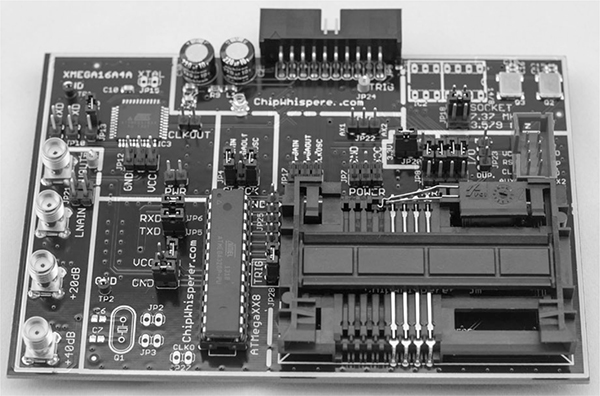
Figure 8-6: MultiTarget Victim Board
The MultiTarget Victim Board is basically three separate systems: an ATmega328, a XMEGA, and a smart card reader. (The ChipWhisperer can perform man-in-the-middle attacks on smart cards, but because cars don’t really use smart cards, we won’t cover that feature here.)
By changing jumpers on the board, you can pass power to enable or disable different systems, but be careful to enable only one section at a time, or you may short the board. Pay attention to the jumper settings before testing.
Installing the Software
First install the ChipWhisperer software. The following instructions are for Linux, but you can find detailed setup instructions for Windows at http://www.newae.com/sidechannel/cwdocs/.
The ChipWhisperer software requires Python 2.7 and some additional Python libraries to run. First, enter the following code:
$ sudo apt-get install python2.7 python2.7-dev python2.7-libs python-numpy
python-scipy python-pyside python-configobj python-setuptools python-pip git
$ sudo pip install pyusb-1.0.0b1
To get the ChipWhisperer software, you can either download a stable version as a ZIP file from the NewAE site or grab a copy from the GitHub repository, as shown here:
$ git clone git://git.assembla.com/chipwhisperer.git
$ cd chipwhisperer
$ git clone git://git.assembla.com/openadc.git
The second git command downloads OpenADC. The OpenADC board of the ChipWhisperer is the oscilloscope part, which measures voltage signals and is basically the heart of the ChipWhisperer system. Use the following commands to set up the software (you should be root in the ChipWhisperer directory):
$ cd openadc/controlsw/python
$ sudo python setup.py develop
$ cd software
$ sudo python setup.py develop
The hardware is already natively supported by Linux, but you should add a group for the normal user that you’ll test so that the user can have access to the device without needing root privileges. To allow non-root users to use the equipment, create a udev file, such as /etc/udev/rules.d/99 -ztex.rules, and add the following to that file:
SUBSYSTEM=="usb", ATTRS{idVendor}=="04b4", ATTRS{idProduct}=="8613",
MODE="0664", GROUP="plugdev"
SUBSYSTEM=="usb", ATTRS{idVendor}=="221a", ATTRS{idProduct}=="0100",
MODE="0664", GROUP="plugdev"
Also, create a file for the AVR programmer called /etc/udev/rules.d/ 99-avrisp.rules:
SUBSYSTEM=="usb", ATTRS{idVendor}=="03eb", ATTRS{idProduct}=="2104",
MODE="0664", GROUP="plugdev"
Now add yourself (you’ll need to log out and back in for these new permissions to take effect):
$ sudo usermod -a -G plugdev <YourUsername>
$ sudo udevadm control -reload-rules
Connect the ChipWhisperer to your machine by plugging a mini-USB cable in to the side of the ChipWhisperer box. The green System Status light on the top should light up, and your ChipWhisperer should now be set up or at least in its unconfigured core.
Prepping the Victim Board
To prep the Victim Board—or device under test (DUT), as it’s referred to in the ChipWhisperer documentation—download the AVR Crypto library (the library isn’t included with the ChipWhisperer framework by default due to export laws) by entering the following:
$ cd hardware/victims/firmware
$ sh get_crypto.sh
We’ll use the AVRDUDESS GUI to program our Victim Board. You can get AVRDUDESS from its GitHub repository at https://github.com/zkemble/avrdudess/ or grab binaries from sites such as http://blog.zakkemble.co.uk/avrdudess-a-gui-for-avrdude/. You’ll need to install mono for this to work:
$ sudo apt-get install libmono-winforms2.0-cil
Next, make sure the Victim Board is set up to use the ATmega328 portion by changing the jumper settings to match the layout in Figure 8-7.
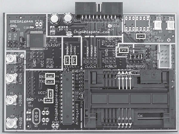
Figure 8-7: Jumper settings for the MultiTarget Victim Board
Your ChipWhisperer should have come with a 20-pin ribbon cable. Plug this cable in to the back of the ChipWhisperer and the USB A/B cable in to the side, as shown in Figure 8-8. Dmesg should report seeing an AVRISP mkII plugged in, which is the programmer that we’ll use to program the target board. This will allow us to perform testing without disconnecting the device.
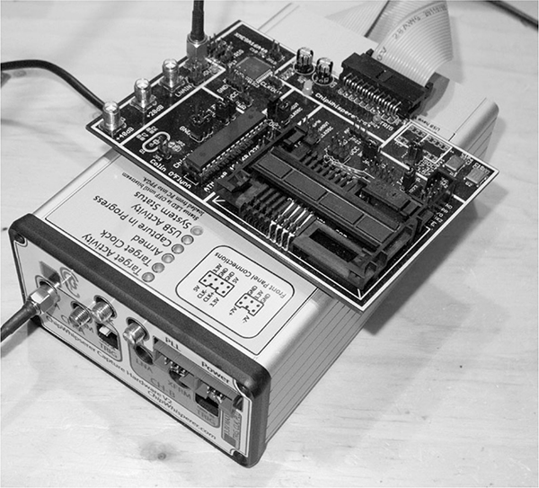
Figure 8-8: Wiring up the MultiTarget Victim Board
Finally, attach the SMA cable from the VOUT on the target board to the LNA connector in CH-A on the front of the ChipWhisperer. Table 8-2 shows the pinout. We’ll use this setup for our demos unless otherwise specified.
Table 8-2: Pinout for the MultiTarget Victim Board
|
Victim Board |
ChipWhisperer |
Component |
|
20-pin connector |
Back of the ChipWhisperer |
20-pin ribbon cable |
|
VOUT |
LNA on CH-A |
SMA cable |
|
Computer |
Side of the ChipWhisperer |
Mini USB cable |
Brute-Forcing Secure Boot Loaders in Power-Analysis Attacks
Now you have your Victim Board set up, we’ll look at using a power-analysis attack to brute-force a password. Power-analysis attacks involve looking at the power consumption of different chipsets to identify unique power signatures. By monitoring the power consumption for each instruction, it’s possible to determine the type of instruction being executed. For instance, a no-operation (NOP) instruction will use less power than a multiply (MUL) instruction. These differences can reveal how a system is configured or even whether a password is correct because a correct password character may use more power than an incorrect one.
In the following example, we’ll explore TinySafeBoot (http://jtxp.org/tech/tinysafeboot_en.htm), a small, open source bootloader designed for AVR systems. The bootloader requires a password in order to make modifications. We’ll use the ChipWhisperer to exploit a vulnerability in its password-checking method and derive the password from the chip. This vulnerability has been fixed in newer versions of TinySafeBoot, but for practice, the old version is included in the victims folder of the ChipWhisperer framework. This tutorial is based on NewAE’s “Timing Analysis with Power for Attacking TSB” (http://www.newae.com/sidechannel/cwdocs/tutorialtimingpasswd.html).
Prepping Your Test with AVRDUDESS
To begin, open AVRDUDESS and select AVR ISP mkII from the Programmer drop-down menu. Make sure you have ATmega328P selected in the MCU field, and then click Detect to verify that you’re connected to the ATmega328p (see Figure 8-9). Select the flash file hardware/victims/firmware/ tinysafeboot-20140331 in the Flash field.
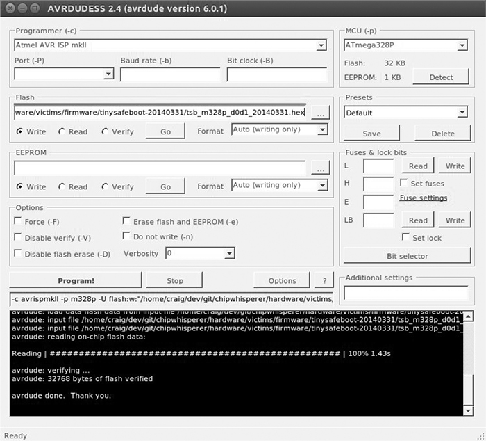
Figure 8-9: Programming TinySafeBoot in AVRDUDESS
Click Program! and AVRDUDESS should write the TinySafeBoot program to the ATmega.
Setting Up the ChipWhisperer for Serial Communications
Now we’re ready for testing! We’ll use the ChipWhisperer to set and monitor the power usage when the bootloader checks for the password. Then, we’ll use this information to build a tool to crack the password much faster than a traditional brute-force method would. To begin, set up the ChipWhisperer to communicate with the bootloader over the bootloader’s serial interface, like this:
$ cd software/chipwhisperer/capture
$ python ChipWhispererCapture.py
The ChipWhisperer has lots of options, so we’ll go step by step through each setting you’ll need to change.
1. In ChipWhispererCapture, go to the General Settings tab and set the Scope Module to ChipWhisperer/OpenADC and the Target Module to Simple Serial, as shown in Figure 8-10.
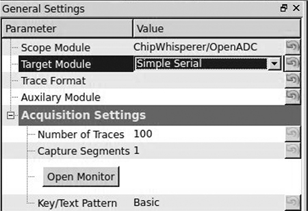
Figure 8-10: Setting the Scope and Target types
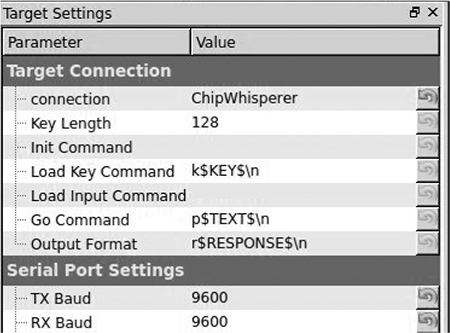
Figure 8-11: Setting Connection and Baud
2. Switch to the Target Settings tab (at the bottom of the window), and change the Connection setting to ChipWhisperer. Then under Serial Port Settings, set both TX Baud and RX Baud to 9600, as shown in Figure 8-11.
3. At the top of the screen, click the red circle next to Scope with DIS in it. The circle should become green and display CON.
4. The ChipWhisperer comes with a simple serial terminal interface. Choose Tools ▸ Open Terminal to open it. You should see a terminal like the one shown in Figure 8-12.
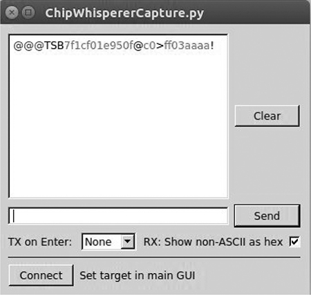
Figure 8-12: ChipWhisperer serial terminal
5. Set TX on Enter at the bottom of the terminal to None, and check the box that says RX: Show non-ASCII as hex (see Figure 8-12). Now click Connect to enable your text areas.
6. Enter @@@ (TinySafeBoot’s start-up password) in the text field to the left of the Send button, and click Send. The bootloader should start with TSB and mainly contain information about the firmware version and AVR settings. TSB is just an identifier used by TinySafeBoot, most likely its initials. The output should match that in Figure 8-12.
Setting a Custom Password
Now we need to set a custom password so that we can monitor the power levels when a password is entered.
First, close the serial terminal. Then enter the following lines in the Python console window, which is at the bottom center of the ChipWhisperer main window.
>>> self.target.driver.ser.write("@@@")
>>> self.target.driver.ser.read(255)
We use the serial command self.target.driver.ser.write("@@@") to send the current password for the bootloader. Next, we enter the serial command self.target.driver.ser.read(255) to read up to the next 255 bytes from the bootloader to see its response to our sending the password (see Figure 8-13).

Figure 8-13: Sending @@@ via ChipWhisperer’s Python console
For convenience, first assign the read and write commands to their own variables so you don’t have to enter such a long command (the following examples assume you’ve completed this step):
>>> read = self.target.driver.ser.read
>>> write = self.target.driver.ser.write
The password is stored in the last page of the device’s flash memory. We’ll grab that page, remove the confirmation ! character from the response, and write a new password—og—to the firmware.
NOTE
You’ll find a more detailed explanation of this procedure in the NewAE tutorials (http://www.newae.com/sidechannel/cwdocs/tutorialtimingpasswd.html) or Python manuals.
Return to the Python console, and enter Listing 8-1.
>>> write('c')
>>> lastpage = read(255)
>>> lastpage = lastpage[:-1]
>>> lastpage = bytearray(lastpage, 'latin-1')
>>> lastpage[3] = ord('o')
>>> lastpage[4] = ord('g')
>>> lastpage[5] = 255
>>> write('C')
>>> write('!')
>>> write(lastpage.decode('latin-1'))
Listing 8-1: Modifying the last page of memory to set the password to og
If the login times out, resend @@@ like so:
>>> write("@@@")
Once you’ve written the new characters to memory, verify that og is the new password with write("og"), followed by a read(255) in the Python console. Notice in Figure 8-14 that we first try sending @@@ but that we don’t get a TinySafeBoot response until we send the og password.
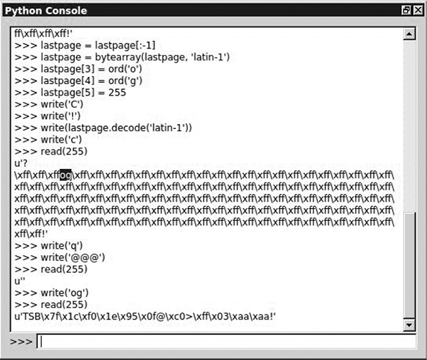
Figure 8-14: Setting the password to og
Resetting the AVR
Having changed the password, we can start reading power signals. First, we need to be able to get out of the infinite loop that the system goes into when we enter an incorrect password. Write a small script to reset the AVR when this happens. While still in the Python console, enter the following commands to create a resetAVR helper function:
>>> from subprocess import call
>>> def resetAVR:
call(["/usr/bin/avrdude", "-c", "avrispmkII", "-p", "m328p"])
Setting Up the ChipWhisperer ADC
Now, set up the ChipWhisperer ADC so that it knows how to record the power trace. Return to the ChipWhisperer main window, click the Scope tab, and set the values as shown in Table 8-3 and Figure 8-15.
Table 8-3: Scope Tab Settings to Set Up the OpenADC for the Victim Board
|
Area |
Category |
Setting |
Value |
|
OpenADC |
Gain Setting |
Setting |
40 |
|
OpenADC |
Trigger Setup |
Mode |
Falling edge |
|
OpenADC |
Trigger Setup |
Timeout |
7 |
|
OpenADC |
ADC Clock |
Source |
EXTCLK x1 via DCM |
|
CW Extra |
Trigger Pins |
Front Panel A |
Uncheck |
|
CW Extra |
Trigger Pins |
Target IO1 (Serial TXD) |
Check |
|
CW Extra |
Trigger Pins |
Clock Source |
Target IO-IN |
|
OpenADC |
ADC Clock |
Reset ADC DCM |
Push button |

Figure 8-15: ADC values to trigger on Serial TX
Monitoring Power Usage on Password Entry
Now we’ll monitor the power usage when entering a password to see whether we can spot a difference in power between a valid and an invalid password. We’ll look at what happens when we enter the now invalid password of @@@. Recall from earlier that when the bootloader detects that you’ve entered a wrong password, it’ll go into an infinite loop, so we can monitor what the power usage looks like at that point. Of course, you’ll need to exit that infinite loop, so once you’ve tried the incorrect password and are sent into a loop, reset the device and try to enter another password. To do this, navigate to the password prompt in the Python console as follows:
>>> resetAVR()
>>> write("@@@")
Now, issue the next command with the correct password, but do not click Enter yet:
>>> write("og")
Click 1 in the green play icon in the toolbar to record one power trace. Immediately after you do so, click Enter in the Python console. A Capture Waveform window should open and show you the power trace recording of the valid password (see Figure 8-16).
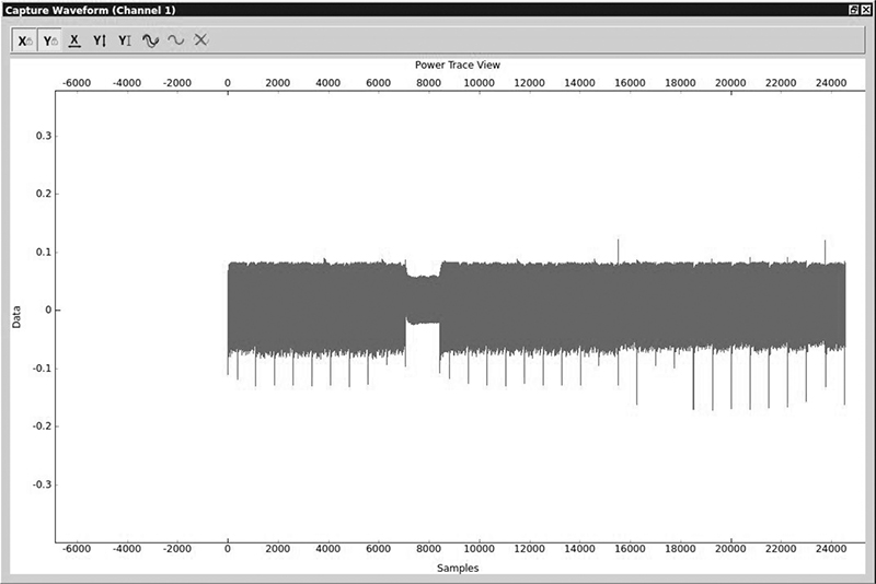
Figure 8-16: Power trace of a valid password
The details of Figure 8-16 aren’t that important; the point is to give you a feel for what a “good” signal looks like. The thick lines you see are normal processing, and there’s a dip around the 8,000 sample range when the processing instructions changed. (This could be something in the password check, but let’s not get hung up on details at this stage.)
Now, enter an invalid password—ff:
>>> resetAVR()
>>> write("@@@")
>>> write("ff")
Figure 8-17 shows the power trace for this password.
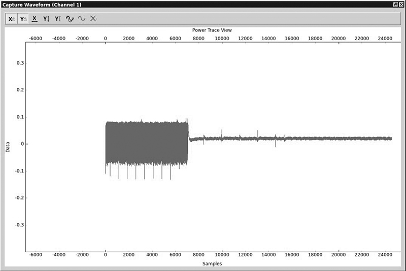
Figure 8-17: Power trace for a password with no valid characters
You can see that the program hangs in its infinite loop when the power reading shifts from normal to a near consistent 0 power usage.
Now, let’s try a password with a valid first character to see whether we notice a difference:
>>> resetAVR()
>>> write("@@@")
>>> write("of")
In Figure 8-18, one additional chunk is active before the device enters the infinite loop. We see normal power usage, followed by the dip at 8,000 that we saw in the first valid reading, and then some more normal usage before the device enters the infinite loop of 0 usage.

Figure 8-18: Power trace of a password with a valid first character
NOTE
You can determine the size of samples used for one valid character by measuring the length between the dip at 8,000 and the infinite loop that starts around 16,000. In this case, we can roughly approximate that the sample size to check one character is about 8,000 traces (16,000 - 8,000).
Scripting the ChipWhisperer with Python
Because the ChipWhisperer is written in Python, it’s highly scriptable, so you can script these power traces to create a brute-forcer that can get the password for the bootloader very quickly. By setting a script to check whether the data points of the power trace exceed a set threshold, your brute-forcer can immediately tell whether the target character is correct. By looking at the data values on the y-axis in Figure 8-18, we can see that when we have activity, data reaches 0.1, but when we’re in the infinite loop, it hovers around the 0 mark. If the target character is correct, the threshold for our script can be set to 0.1, and if no data in the sample range of a byte reaches 0.1, then we can conclude that we’re in the infinite loop and the password character was incorrect.
For example, if the password is made up of 255 different characters with a maximum length of 3, the password will be one of 2553, or 16,581,375, possibilities. However, because we can instantly detect when we have a correct character, in a worst-case scenario, the brute-forcer will have to try only 255 × 3, or 765, possibilities. If the character doesn’t match the set password, the bootloader jumps into the infinite loop. On the other hand, if the password check routine waited until the entire password was checked regardless of its correctness, this type of timing analysis couldn’t be done. The fact that the small code on embedded systems is often designed to be as efficient as possible can open it up to devastating timing attacks.
NOTE
For details on how to write your own brute-forcer for the ChipWhisperer, see the NewAE tutorials. A sample brute-forcer is included at http://www.nostarch.com/carhacking/.
Secure bootloaders and any embedded system that checks for a valid code can be susceptible to this type of attack. Some automotive systems require a challenge response or a valid access code to access lower-level functions. Guessing or brute-forcing these passwords can be very time consuming and would make traditional brute-forcing methods unrealistic. By using power analysis to monitor how these passwords or codes are being checked, you can derive the password, making something that would’ve been too time consuming to crack completely doable.
Fault Injection
Fault injection, also known as glitching, involves attacking a chip by disrupting its normal operations and potentially causing it to skip running certain instructions, such as ones used to enable security. When reading a chip’s data sheet, you’ll see that attached to the range for clock speeds and power levels is a warning that failing to stick to these ranges will have unpredictable results—and that’s exactly what you’ll take advantage of when glitching. In this section, you’ll learn how to introduce faults by injecting faults into clock speeds and power levels.
Clock Glitching
Any ECU or chip will rely on an internal clock to time its instructions. Each time the microcontroller receives a pulse from the clock, it loads an instruction, and while that instruction is being decoded and executed, the next instruction is being loaded. This means that a steady rhythm of pulses is needed for the instructions to have time to load and execute correctly. But what happens if there’s a hiccup during one of these clock pulses? Consider the clock glitch in Figure 8-19.
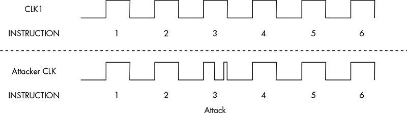
Figure 8-19: Normal clock cycle (top) and glitched clock cycle (bottom)
Because the Program Counter has time to increment but not enough time to decode and execute the instruction before the next instruction is loaded, the microcontroller will usually skip that instruction. In the bottom cycle of Figure 8-19, instruction 3 is skipped because it does not have enough time to execute before another instruction is issued. This can be useful for bypassing security methods, breaking out of loops, or re-enabling JTAG.
To perform a clock glitch, you need to use a system faster than your target’s system. A field-programmable gate array (FPGA) board is ideal, but you can accomplish this trick with other microcontrollers, too. To perform the glitch, you need to sync with the target’s clock, and when the instruction you want to skip is issued, drive the clock to ground for a partial cycle.
We’ll demonstrate a clock-glitching attack using the ChipWhisperer and some demo software made for this kind of attack. The Victim Board setup is almost the same as for the power attack, except that you’ll need to change the jumpers for the Clock pin (in the middle of the board), which should be set only for FPGAOUT by jumping the pins (see Figure 8-20).
Figure 8-20: MultiTarget Victim Board set for glitching
We’ll set up the ChipWhisperer to control the clock of the ATmega328. Both the general settings and the target settings are the same as in the power attack discussed in “Setting Up the ChipWhisperer for Serial Communications” on page 140; the only exception is that we’ll set the baud rate to 38400 for both TX and RX. Enable both the Scope and Target by switching from DIS to CON in the toolbar, as discussed earlier. Figure 8-21 and Table 8-4 show the complete settings.
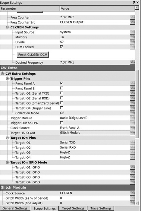
Figure 8-21: Scope settings for glitching
Table 8-4: ChipWhisperer Main Window Settings for a Clock-Glitch Attack
|
Area |
Category |
Setting |
Value |
|
OpenADC |
ADC Clock |
Frequency Counter Src |
CLKGEN Output |
|
OpenADC |
CLKGEN Settings |
Desired Frequency |
7.37 MHz |
|
OpenADC |
CLKGEN Settings |
Reset CLKGEN DCM |
Push button |
|
Glitch module |
Clock Source |
CLKGEN |
|
|
CW Extra |
Trigger Pins |
Target HS IO-Out |
Glitch Module |
These settings give the ChipWhisperer full control of the target board’s clock and allow you to upload the glitch demo firmware. You’ll find the firmware for the target in the ChipWhisperer framework in this directory: hardware/victims/firmware/avr-glitch-examples. Open glitchexample.c in your favorite editor and then go to the main() method at the bottom of the code. Change glitch1() to glitch3() in order to follow along with this demo, and then recompile the glitchexample firmware for the ATmega328p:
$ make MCU=atmega328p
Now, upload the glitchexample.hex file via AVRDUDESS, as we did in “Prepping Your Test with AVRDUDESS” on page 139. Once the firmware is loaded, switch to the main ChipWhisperer window and open a serial terminal. Click Connect, and then switch to AVRDUDESS and click Detect. This should reset the chip so that you see hello appear in the capture terminal. Enter a password, and click Send. Assuming you enter the wrong password, the capture terminal should display FOff and hang, as shown in Figure 8-22.
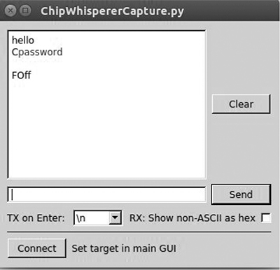
Figure 8-22: A bad password example
Now return to your editor and look at the glitchexample source code. As shown in Listing 8-2, this is a simple password check.
for(cnt = 0; cnt < 5; cnt++){
if (inp[cnt] != passwd[cnt]){
passok = 0;
}
}
if (!passok){
output_ch_0('F');
output_ch_0('O');
output_ch_0('f');
output_ch_0('f');
output_ch_0('\n');
} else {
output_ch_0('W');
output_ch_0('e');
output_ch_0('l');
output_ch_0('c');
output_ch_0('o');
output_ch_0('m');
output_ch_0('e');
output_ch_0('\n');
}
Listing 8-2: Password check method for glitch3()
If an invalid password is entered, passok is set to 0, and the message Foff is printed to the screen; otherwise, Welcome is printed to the screen. Our goal is to introduce a clock glitch that bypasses the password verification either by skipping over the instruction that sets passok to 0 (so that it’s never set to 0) or by jumping straight to the welcome message. We’ll do the latter by manipulating the width and offset percentages in the glitch settings.
Figure 8-23 shows some possible places to locate the glitch. Different chips and different instructions react differently depending on where your glitch is placed, so experiment to determine which location works best for your situation. Figure 8-23 also shows what a normal clock cycle looks like under a scope. If we use a positive offset in the ChipWhisperer settings, it’ll cause a brief drop in the middle of the clock cycle. If we use a negative offset, it’ll cause a brief spike before the clock cycle.
We’ll set the following glitch options in the ChipWhisperer to cause a brief spike before the clock cycle by using a -10 percent offset:
Glitch width %: 7
Glitch Offset %: -10
Glitch Trigger: Ext Trigger: Continuous
Repeat: 1
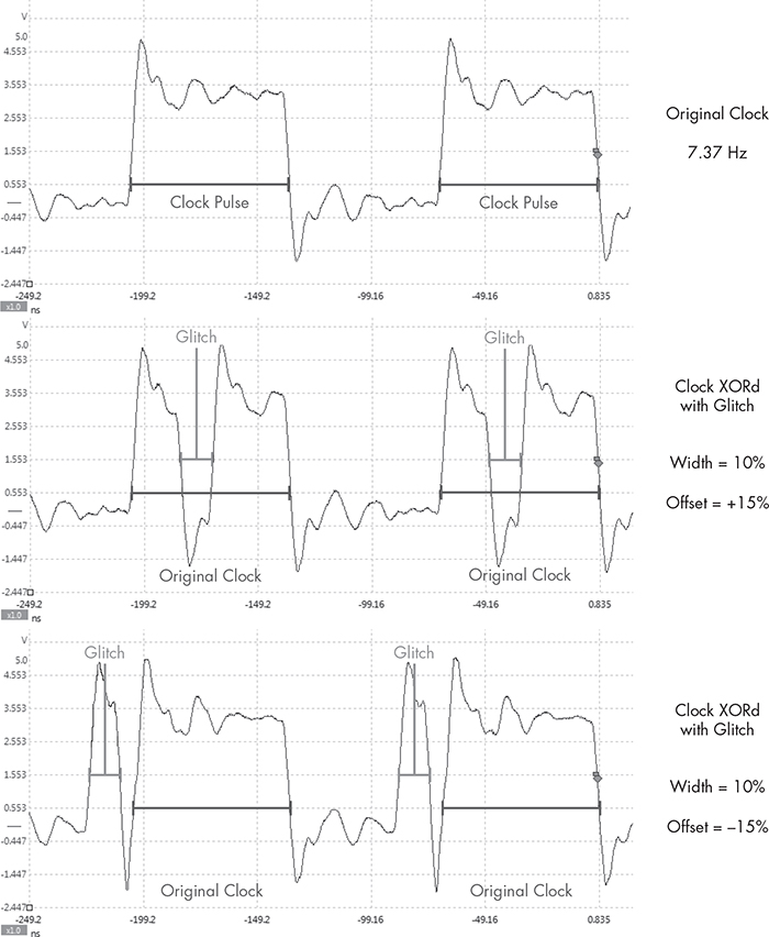
Figure 8-23: Example glitch placements
Now return to the ChipWhisperer main window to set up the CW Extras, as shown in Figure 8-24. This will configure the ChipWhisperer to cause the clock glitch only when it gets a signal from the trigger line.
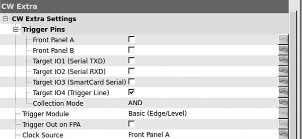
Figure 8-24: Glitch setup in the CW Extra Settings
NOTE
Glitching is an inexact science. Different chips will respond to settings differently, and you’ll need to play around with settings a lot to get the timing right. Even if you fail to exploit the clock glitch consistently, often you’ll need to get it right only once to exploit a device.
Setting a Trigger Line
Now that we have the ChipWhisperer set up to listen for a signal on the trigger line, we need to modify the code to use the trigger line. The trigger line is pin 16 on the ChipWhisperer connector. When the trigger line receives a signal (voltage peaks), it triggers the ChipWhisperer software to spring into action.
The trigger line is a generic input method used by ChipWhisperer. The goal is to get the trigger line to receive a signal just before the point we want to attack. If we were looking at a piece of hardware and noticed a light come on just before the area we wanted to attack, we could solder the LED to the trigger line in order to make the ChipWhisperer wait until just the right moment.
For this demo, we’ll modify the firmware to make the trigger line go off in the area we want to glitch. First we’ll add some code to the default glitch 3 example shown in Listing 8-2. Use your favorite editor to add the defines in Listing 8-3, toward the top of the glitchexample.c.
#define trigger_setup() DDRC |= 0x01
#define trigger_high() PORTC |= 0x01
#define trigger_low() PORTC &= ~(0x01)
Listing 8-3: Setting up trigger defines in glitchexample.c
Place a trigger_setup() inside the main() method just before it prints hello, and then wrap your target with the trigger, as shown in Listing 8-4.
for(cnt = 0; cnt < 5; cnt++){
if (inp[cnt] != passwd[cnt]){
trigger_high();
passok = 0;
trigger_low();
}
}
Listing 8-4: Adding trigger_high and trigger_low around passok to trigger a glitch
Now, recompile make MCU=atmega328p, and reupload the firmware to the Victim Board. (Make sure to set the Glitch Trigger option to Manual in the ChipWhisperer settings before you upload the firmware or you may accidentally glitch the firmware upload.) Once the firmware is uploaded, switch the Glitch Trigger option back to Ext Trigger:Continous. Now, enter any password. If you get a Welcome message, you’ve successfully glitched the device, as shown in Figure 8-25.

Figure 8-25: Successfully glitching password check
Unfortunately, in the real world, you probably won’t be able to use a trigger line in the same way because you won’t have access to the target source or a trigger event won’t be close enough to where you want to glitch. In such cases, you’ll need to play with other settings and the Ext trigger offset. Open the Glitch Monitor under Tools to experiment with different settings.
Power Glitching
Power glitching is triggered like clock glitching: you feed the target board the proper power at a steady rate, and when you want to trigger unexpected results at particular instructions, you either drop or raise the voltage to interrupt that instruction. Dropping the voltage is often safer than raising it, so try that first. Each microcontroller reacts differently to power glitching, so play around at different points and power levels to build a glitch profile and see what types of behavior can be controlled. (When instructions are skipped via power glitching, it’s often because the opcode instruction has become corrupted and done something other than the intended instruction or because one of the registers has become corrupted.)
NOTE
Some microcontrollers aren’t vulnerable at all to power glitching, so test with your target chipset before trying it on a vehicle.
Power glitching can also affect memory reads and writes. Depending on which instruction is running during the power fault, you can cause the controller to read the wrong data or forget to write a value.
Invasive Fault Injection
Because invasive fault injection attacks are more time-consuming and expensive than glitch attacks, we’ll examine them only briefly here. However, if you need to do the job and you have the resources, invasive fault injection is often the best way. The catch is that it doesn’t preserve the target and can even destroy it.
Invasive fault injection involves physically unpacking the chip, typically with acid (nitric acid and acetone) and using an electron microscope to image the chip. You can work on just the top or bottom layer of the chip or map out each layer and decipher the logic gates and internals. You can also use microprobes and a microprobe station to inject the exact signal you want into your target. By the same token, you could use targeted lasers or even directed heat to cause optical faults to slow down processes in that region. For instance, if a move instruction is supposed to take two clock cycles, you can slow the registry retrieval to make it late for the next instruction.
Summary
In this chapter, you’ve learned several advanced techniques for attacking embedded systems; these techniques will become only more valuable as automotive security improves. You learned how to identify chips and monitor power usage to create a profile of good operations. We tested whether password checks could be attacked by monitoring the power output of bad characters in passwords, ultimately to create a brute-forcing application using power analysis to cut the password brute-force time down to seconds. We also saw how clock and power glitching can make instructions skip at key points in the firmware’s execution, such as during validation security checks or when setting JTAG security.